
The essential answer
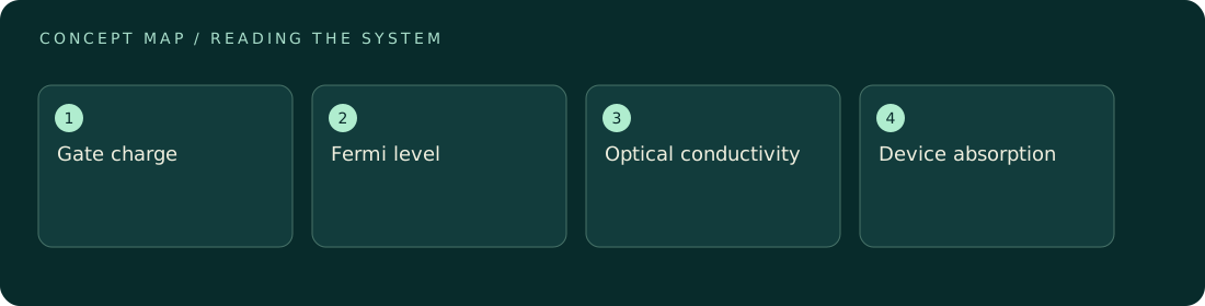
Gating changes graphene's carrier density and Fermi level, which changes its optical conductivity and therefore absorption, reflection, or transmission in an optical structure. At appropriate photon energies, Pauli blocking can suppress interband absorption; at lower frequencies, intraband and plasmonic responses can be important. The result depends on geometry, frequency, scattering, temperature, and the surrounding optical stack. Gate-controlled optical modulation is a material response, not evidence that electrical bias creates unaccounted momentum. Include electrode forces and heating in any coupled force experiment.
How to reason about it
A simple capacitor model relates induced sheet charge to gate voltage relative to the charge-neutrality point, but trapped charge, quantum capacitance, and dielectric properties can modify that relation. Optical behavior is often modeled with a complex sheet conductivity coupled to Maxwell boundary conditions. Patterning and cavities can enhance interaction, so a large device-level absorption change should not be assigned to a bare isolated sheet without context. In a simplified low-temperature interband picture, transitions become blocked when photon energy is below about twice the magnitude of Fermi energy, with finite temperature and scattering broadening the threshold. Real measurements require independent electrical characterization and optical normalization. Gate leakage can heat the sample, while changing voltage alters capacitive forces even in the dark. Compare illuminated and dark voltage sweeps and measure outgoing optical power to separate these channels before interpreting a mechanical response.
ILLUSTRATIVE · NOT A REPORTED RESULT
An example to work through
Assume an illustrative photon energy of 0.80 eV and an idealized low-temperature graphene model. The simple Pauli-blocking threshold is |EF| above 0.40 eV. Moving from 0.20 eV to 0.50 eV crosses that threshold and can reduce interband absorption, but it does not specify the total device transmission because intraband loss and the optical stack remain. Separately, if an electrode force is proportional to V², changing gate voltage from 2 V to 4 V quadruples that force. Optical and mechanical changes can therefore occur together for different reasons.
Where interpretation fails
Do not infer Fermi level directly from nominal gate voltage without a capacitance and offset model. Nor should an absorption result for patterned graphene in a resonator be generalized to an unpatterned sheet at another wavelength. Gate hysteresis and leakage can create misleading correlations with optical or force signals.
The next decision
Use graphene gating when the operating frequency and device geometry support a characterized conductivity change. Measure electrical state, leakage, temperature, and optical outputs under the same sweep. For force studies, bound dark electrostatic effects and compare the observed load with the changed optical momentum budget before proposing an additional mechanism.
Sources & context
These sources support the concepts noted below. Our synthetic examples and research framing are educational interpretation; they are not findings from these organizations or validation of our ventures.
- Kim et al.: Electronically Tunable Perfect Absorption in Graphene ↗
Gate-controlled optical absorption in structured graphene; PDF abstract and opening text checked.
Source check: Relevant excerpt or resource metadata checked; see support note. Original illustrative calculation, not source data.
Educational research context, not a validated device specification or clinical protocol. Read our editorial and correction policy.